
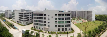
Sam Fenwick visited Hytera’s factory and headquarters in Shenzhen to learn more about how the company’s two-way radios are made

The day begins with a downpour, followed by a coach journey through lush vegetation broken up with massive high-rise apartments that sprout up like giant angular mushrooms and misty mountains. Twenty-four years ago, a seed was planted into this fertile soil, growing to become one of the biggest manufacturers of two-way radios in the world.
I’m in China for a tour of Hytera’s manufacturing plant in Shenzhen. We don pink overalls and blue shoe protectors before being ushered into an airlock and blasted with jets of air. Taveevong Pongprasertsuk, Hytera’s engineering director, escorts the party from one glowing white room to the next, starting with an inspection area for incoming components, which are sampled and checked according to American quality standards. He then takes us to a component storage facility, filled with shelves, each containing what seem to be white plastic discs, all carefully barcoded. The barcodes coupled with PDA devices are used to ensure a first-in, first-out approach to stock control. Some of the components are so sensitive that they need to be kept in foil bags and stored in special cabinets.
Pongprasertsuk shows us a machine that laser engraves serial numbers onto circuit boards to ensure that they can be tracked all the way through the manufacturing process, before quickly moving onto the SMT (surface mount technology) machines that allow the bulk of the components to be soldered onto the circuit boards. The boards are then inspected, baked and then inspected again, in a lead-free process. Some of the components cannot be soldered using SMT, so Hytera makes use of selective wave soldering to attach these components. The lines here can print more than one million printed circuit boards (PCBs) a month.

The partial use of automation allows Hytera’s Shenzhen factory to produce more than one million PCBS a month and around four million handsets a year
We go up to the third floor, where we see the assembly of the analogue TC310 handset under way, and are ushered into a laboratory where environmental testing is carried out. Here, cables bob up and down in a hypnotic manner with weights attached, and a small white plastic dome tirelessly strokes a keypad. There is also a chamber that can handle temperatures between -70°C and 150°C – allowing equipment to be tested for extremes of cold, heat and humidity. We then move to a partially automated line, where the human operators are responsible for cleaning and inspecting the components, a very small conveyor belt slowly moving the terminals along until they are complete. Pongprasertsuk adds that roughly four million handsets are made here every year.
He points out that the complex isn’t just a factory – it’s also a home to 2,000 workers, complete with two basketball courts. There is a sense of order thanks to a dress code, with different colour clothing for different types of staff, which allows managers and staff to quickly recognise each other’s roles. This is especially useful when dealing with newly trained personnel, who naturally require more guidance than their more experienced peers, and when or if something occurs that needs to be brought to a manager’s attention.
We then move onto the fourth floor, which is dedicated to base station assembly. Pongprasertsuk explains that while it is currently done by hand, the intention is to make the process more automated. That doesn’t mean that the quantities here are small by any means; roughly a million base stations pass through the factory gates every year. We pass racks of spectrum analysers, a room where accelerated life testing is performed at 50°C, and move into the factory acceptance testing area, where towers full of RF equipment are tested for transmission and functionality.
We head to Hytera’s headquarters. A whistle-stop tour of its training facilities then follows – they are for both Hytera’s staff and its customers. The room set aside for the former has a wall dominated by photos of 146 master trainers, while the rooms for customer training cover both system installation and configuration.
The tour moves onto the exhibition hall which displays Hytera’s range of products, including an RFID reader for terminals, which allows security personnel to provide their location information in real time just by tapping a pad. I’m told that one of the main messages Hytera is looking to make is that “digital doesn’t have to be expensive” and that it can be delivered at the same price as analogue technology. Another interesting set-up is a command vehicle capable of catering for a wide scope of wireless protocols and providing a 7km range in urban conditions. It could also be used to stream video feeds from users in the field.
A surprise is in store for us over in the infrastructure section: E-pack100, a DMR Tier-II based mesh-network node that can be also be used as a radio using a remote speaker microphone or a conventional repeater. Another product that is on show but has yet to hit the shelves is the DMR Trunking Cube, a DMR Tier III self-contained IP67-rated base station that weighs less than 26kg and is designed to provide flexible coverage, be it box-, wall-, vehicle- or outdoor-mounted. It supports multi-carrier and software-defined radio technology, the latter allowing the frequencies to be easily configured, and has 50kHz minimum channel spacing.
The day was an eye-opening experience and I know that next time I hold a radio handset, I’ll have a new appreciation of all the work and dedication required to take it all the way from the drawing board to the palm of my hand.

